W5B03A-1720DFV1 Module Specification
1 Product Description
W5B03A-1720DF-1624 (hereinafter referred to as: W5B03A) is a module based on Realtek's highly integrated chip RTL8720DF which supports WLAN dual-band (2.4GHz and 5GHz) and low-power Bluetooth 5.0. The chip is built-in Real-M300 (or KM4) high performance MCU (Armv8-M, compatible with Cortex-M33 instruction set), Real-M200 (or KM0) low power MCU (Armv8-M, compatible with Cortex-M23 instruction set), WLAN (802.11a/b/g/n) MAC, support for 1T1R WLAN baseband, RF, and Bluetooth. A set of configurable GPIO ports are provided for the control of different peripheral devices, and an internal memory is integrated to support simple application development for full Wi-Fi and BT 5.0 protocol functionality.
1.1 Product Features
- Built-in low power consumption KM4 MCU, which can be used as an application processor.
- 200MHz main frequency support
- Operating voltage: 3.0V~3.6V
- Support 802.11 a/b/g/n, 2.4GHz and 5GHz.
- Support HT20/HT40 mode
- Support BLE5.0
- Support Low Power Beacon Listening Mode
- WIFI/BT shared antenna
- Built-in AES/DES/FSHA hardware engine
- Support TrustZone-M secure boot
- Support STA/AP/STA+AP working mode
- Operating temperature: -20℃ to 85℃ or -40℃ to 105℃ (according to ordering information)
1.2 Specification
| Item | Description |
|---|---|
| Product Name | W5B03A-1720DF |
| Product Description | Wi-Fi 2.4GHz/5GHz and BLE 5.0 Dual-Mode Dual-Band Module |
| Interface Type | SMT Type |
| Eco-Friendly | All hardware components are fully compliant with the EU RoHS Directive |
1.3 Absolute Electrical Parameters
| Parameter | Description | Minimum | Maximum | Unit |
|---|---|---|---|---|
| Ts | Storage Temperature | -40 | 125 | °C |
| VBAT | Supply Voltage | 3.0 | 3.6 | V |
| Electrostatic Discharge Voltage (Human Body Models) | TAMB -25 °C | -2 | 2 | KV |
| Electrostatic Discharge Voltage (Device Models) | TAMB -25°C | -500 | 500 | 500 |
1.4 Normal operating conditions
| Parameter | Description | Minimum | Standard | Maximum | Unit |
|---|---|---|---|---|---|
| Ta | Operating Temperature | -20 | - | 85 | °C |
| Ta | Operating Temperature | -40 | - | 105 | ℃ |
| VD33 | Supply Voltage | 3.0 | 3.3 | 3.6 | V |
| V-OL | IO output low voltage | - | - | 0.4 | V |
| V-OH | IO Output High Voltage | 2.4 | - | - | - |
| V-IL | IO Input Low Voltage | - | - | - | 0.8 |
| V-IH | IO Input High Voltage | 2.0 | - | - | V |
| I-IL | Input Leakage Current | -10 | ±1 | 10 | uA |
2 Pin Description
2.1 Pin Definition Diagram & Pin Definition
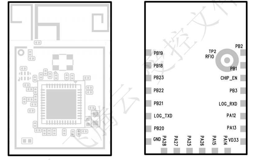
| Serial Number | Pin Definition | IO Type | Function |
|---|---|---|---|
| 1 | PB2 | I/O | GPIOB_2/UART_RXD |
| 2 | PB1 | I/O | GPIOB_1/UART_TXD |
| 3 | CHIP_EN | I | High: Enable the chip. Low: Module power off. |
| 4 | PB3 | I/O | GPIOB_3/SWD_CLK |
| 5 | LOG_RXD | I/O | GPIOA_8/UART_LOG_RXD |
| 6 | PA12 | I/O | GPIOA_12/SPI_MOSI |
| 7 | PA13 | I/O | GPIOA_13/SPI_MISO |
| 8 | VD33 | P | Power Supply 3.3V |
| 9 | PA14 | I/O | GPIOA_14/SPI_CLK/UART_RTS |
| 10 | PA15 | I/O | GPIOA_15/SPI_CS/UART_CTS |
| 11 | PA26 | I/O | GPIOA_26/HSDP |
| 12 | PA25 | I/O | GPIOA_25/HSDM |
| 13 | PA27 | I/O | GPIOA_27/SWD_DAT |
| 14 | PA28 | I/O | GPIOA_28/RREF |
| 15 | GND | P | GND |
| 16 | PB20 | I/O | GPIOB_20/SDIO_CMD |
| 17 | LOG_TXD | I/O | GPIOA_7/UART_LOG_TXD |
| 18 | PB21 | I/O | GPIOB_21/SDIO_CLK |
| 19 | PB22 | I/O | GPIOB_22/SDIO_D0 |
| 20 | PB23 | I/O | GPIOB_23/SDIO_D1 |
| 21 | PB18 | I/O | GPIOB_18/SDIO_D2 |
| 22 | PB19 | I/O | GPIOB_19/SDIO_D3 |
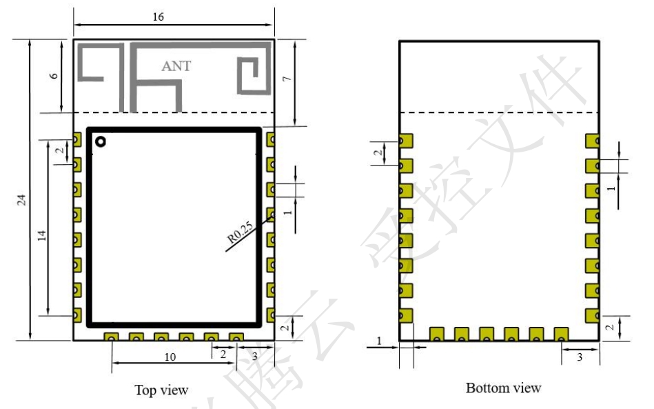
3 Package Information and Production Guidelines
3.1 Mechanical Dimensions
PCB size:16±0.3mm (L)×24±0.3mm (W) ×0.8±0.1mm (H)。单位:mm