RTL8711DCM and MCU Interface Design Guide
Phaten IoT RTL8711DCM Module Hardware Interface Configuration and MCU Interaction Complete Reference Documentation
Overview
This document provides detailed information about the RTL8711DCM WiFi module hardware interface design with host MCU and SOC, including UART communication, I2S audio interface, GPIO control and other key functions pin configuration and circuit design reference.
1. Hardware Interface Reference Schematic
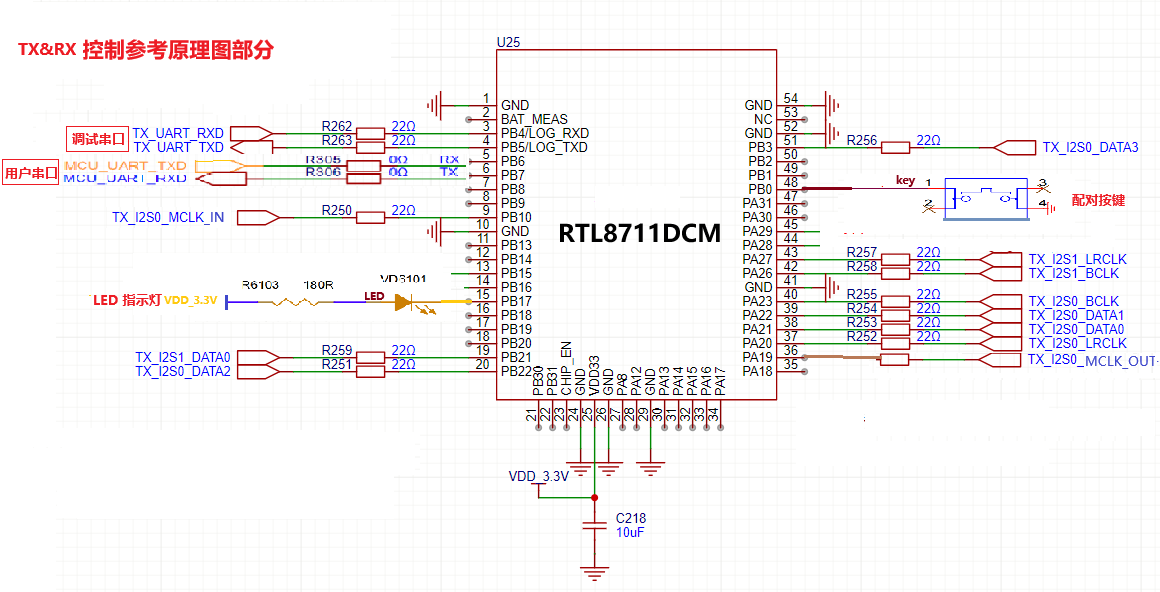
2. Core Function Interface Configuration
2.1 Debug UART Interface
The RTL8711DCM module provides dedicated debug UART for system log output and development debugging.
| Module Pin | Function Definition | Description |
| PB4 | UART_LOG_RX | Debug UART receive |
| PB5 | UART_LOG_TX | Debug UART transmit |
2.2 MCU Communication UART Interface
Primary data communication interface between RTL8711DCM and external MCU.
| Module Pin | Function Definition | Description |
| PB6 | UART_TX | MCU communication transmit |
| PB7 | UART_RX | MCU communication receive |
2.3 User Control Interface
| Module Pin | Function Definition | Description |
| PB0 | Pairing Button | WiFi pairing/reset function button |
2.3.2 LED Status Indicator
| Module Pin | Function Definition | Description |
| PB17 | LED Indicator | Module working status indicator |
3. I2S Audio Interface Configuration
RTL8711DCM supports dual I2S audio input, suitable for stereo audio capture applications.
3.1.1 Master Clock Signal
| Module Pin | Signal Definition | Function Description |
| PB10 | I2S_IN_MCLK | I2S input master clock signal |
| Module Pin | Signal Definition | Function Description |
| PA23 | I2S0_IN_BCLK | First channel bit clock signal |
| PA20 | I2S0_IN_LRCLK | First channel left/right clock |
| PA21 | I2S0_IN_DATA0 | First channel data line 0 |
| PA22 | I2S0_IN_DATA1 | First channel data line 1 |
| PB22 | I2S0_IN_DATA2 | First channel data line 2 |
| PB23 | I2S0_IN_DATA3 | First channel data line 3 |
| Module Pin | Signal Definition | Function Description |
| PA26 | I2S1_IN_BCLK | Second channel bit clock signal |
| PA27 | I2S1_IN_LRCLK | Second channel left/right clock |
| PB21 | I2S1_IN_DATA0 | Second channel data line 0 |
3.2 I2S Audio Output Interface (RX)
RTL8711DCM provides I2S audio output function, supporting multi-channel audio playback.
3.2.1 Master Clock Signal
| Module Pin | Signal Definition | Function Description |
| PA19 | I2S_OUT_MCLK | I2S output master clock signal |
3.2.2 I2S Output Signal Group
| Module Pin | Signal Definition | Function Description |
| PA23 | I2S0_OUT_BCLK | Output bit clock signal |
| PA20 | I2S0_OUT_LRCLK | Output left/right clock |
| PA21 | I2S0_OUT_DATA0 | Output data line 0 |
| PB18 | I2S0_OUT_DATA1 | Output data line 1 |
| PB19 | I2S0_OUT_DATA2 | Output data line 2 |
| PB20 | I2S0_OUT_DATA3 | Output data line 3 |
Part Two: RTL8711DCM and SOC Amplifier Integrated Design
4. SOC Amplifier Integrated Design Solution
4.1 Audio Transmit (TX) Reference Design
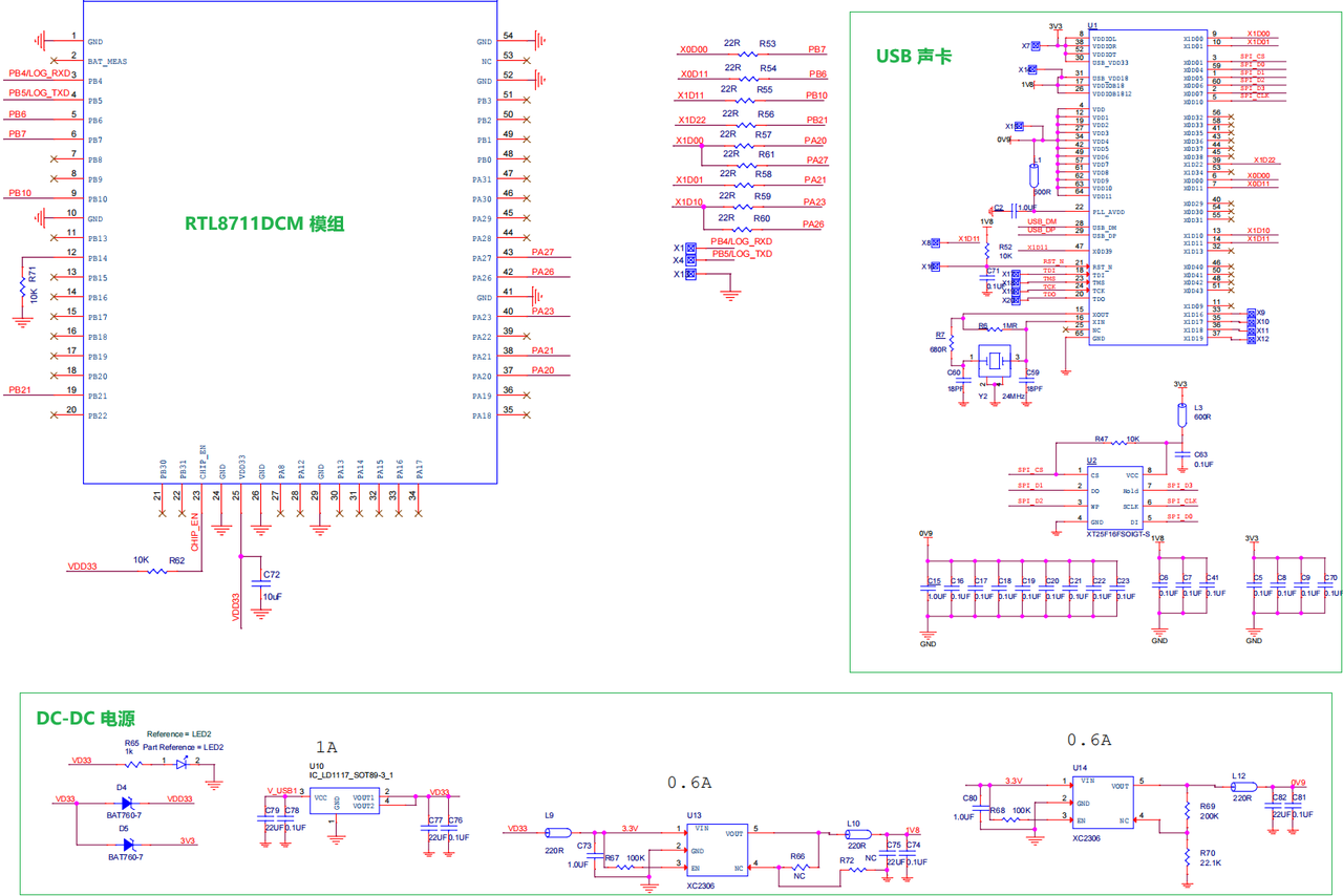
4.1.1 Power Management System
RTL8711DCM audio transmit end adopts multi-level power management solution to ensure stable system operation.
DC-DC Power Configuration
| Power Chip | Output Voltage | Power Supply Target | Function Description |
| LD1117 | 3.3V LDO | Module and USB sound card | Linear regulator, low noise |
| DC-DC XC2036 | 1.8V/0.9V | USB sound card | Switching power supply, high efficiency |
RTL8711DCM transmit end I2S-TDM interface configuration, supporting high-quality audio transmission.
| Module Pin | Signal Definition | Function Description |
| PB10 | I2S_IN_MCLK | I2S input master clock signal |
| PA23 | I2S0_IN_BCLK | First channel bit clock signal |
| PA20 | I2S0_IN_LRCLK | First channel left/right clock |
| PA21 | I2S0_IN_DATA0 | First channel data line 0 |
4.1.3 TX End UART Interface
Debug UART
| Module Pin | Function Definition | Description |
| PB4 | UART_LOG_RX | Debug UART receive |
| PB5 | UART_LOG_TX | Debug UART transmit |
MCU Communication UART
| Module Pin | Function Definition | Description |
| PB6 | UART_TX | MCU communication transmit |
| PB7 | UART_RX | MCU communication receive |
4.2 Audio Receive (RX) Reference Design
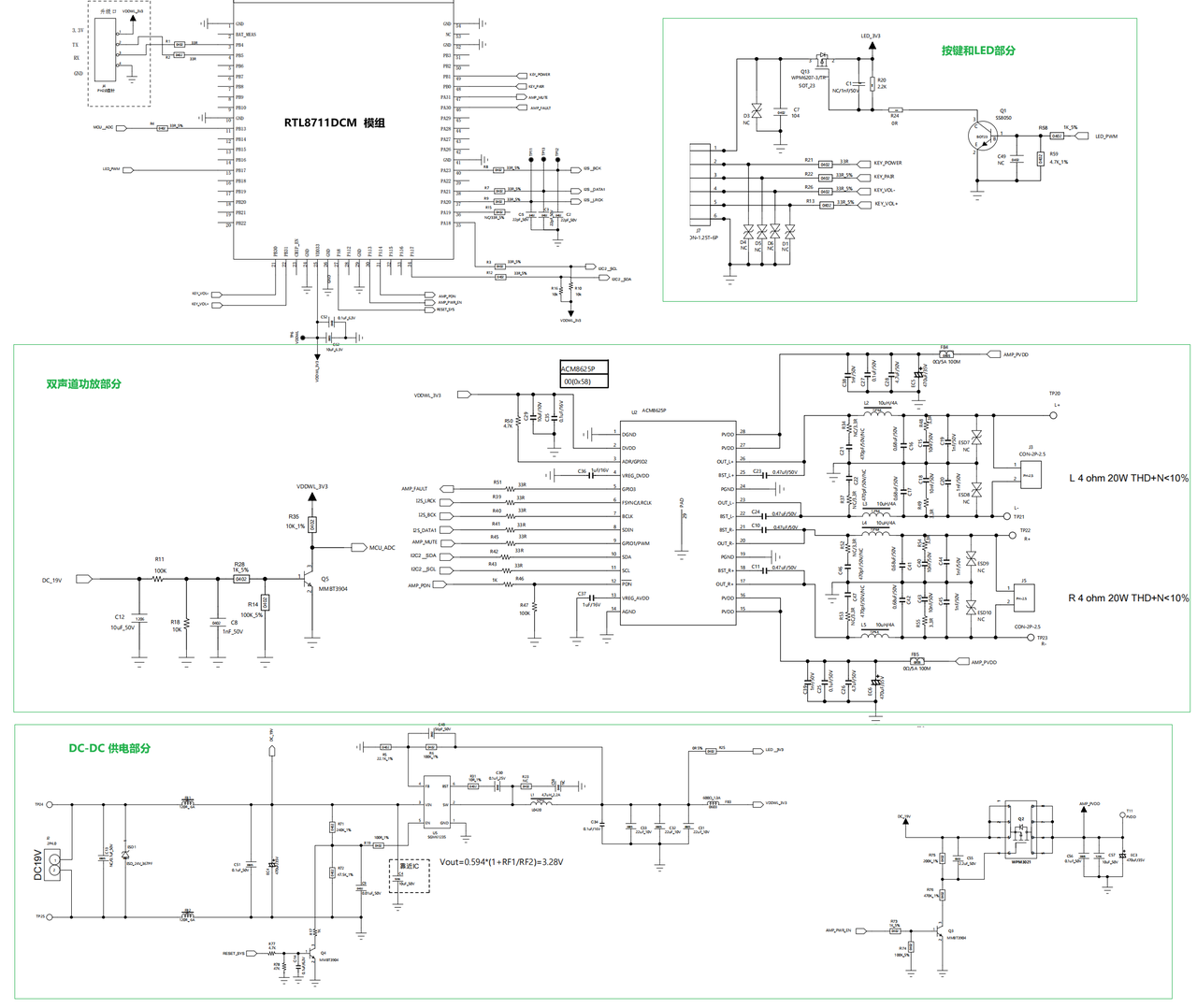
4.2.1 Power System Configuration
RTL8711DCM audio receive end power system design, supporting speaker amplifier applications.
Power Configuration Solution
| Power Type | Output Specification | Power Supply Target | Application Description |
| AC-DC Switching Power Supply | 19V DC | Speaker system | Main power supply |
| DC-DC Converter | 3.3V | RTL8711DCM module | Module working power |
4.2.2 User Control Interface
RTL8711DCM receive end provides button and LED indicator interfaces for user interaction and status indication.
| Module Pin | Function Definition | Description |
| PB0 | Pairing Button | WiFi pairing/reset function |
| PB1 | Power Button | Device power switch control |
| PB30 | Volume Up Button | Volume increase control |
| PB31 | Volume Down Button | Volume decrease control |
| PB17 | LED Indicator | Device status indicator |
4.2.3 Amplifier Drive Control
RTL8711DCM integrates ACM8625P amplifier chip control interface to achieve high-quality audio output.
I2C Control Interface
| Module Pin | Signal Definition | Function Description |
| PB8 | I2C-SDA | Amplifier chip data line |
| PB9 | I2C-SCL | Amplifier chip clock line |
I2S Audio Data Interface
| Module Pin | Signal Definition | Function Description |
| PA20 | I2S_LRCK | Left/right channel clock signal |
| PA21 | I2S_DATA | Audio data signal |
| PA23 | I2S_BCK | Bit clock signal |
Amplifier Control Signals
| Module Pin | Signal Definition | Function Description |
| PB2 | AMP_PWR_EN | Amplifier power enable (active high) |
| PA30 | AMP_FAULT | Amplifier fault status detection |
| PA31 | AMP_MUTE | Amplifier mute control |
| PB20 | AMP_PDN | Amplifier power down control |